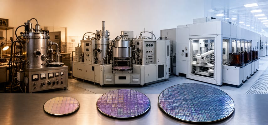
History of Applied Materials
Introduction — solving a manufacturing puzzle that the industry took for granted
Applied Materials began with a deceptively simple problem: how to place atom-thin layers of metal and dielectric onto silicon wafers in a way that was repeatable, uniform and fast enough to support commercial semiconductor production. That technical constraint—how to control matter at the surface of a wafer—was the bottleneck behind shrinking transistors and rising chip yields. Applied Materials turned that bottleneck into a business by selling the machines that do the work.
Over subsequent decades the company grew from a niche capital-equipment supplier into one of the foundational firms of the semiconductor supply chain, shaping not only process tools but also the economics of chip scaling, thin-film displays and later packaging and services. For example, Applied developed successive generations of equipment as wafers grew larger and later invested in tools supporting the industry’s transition from 200-mm to 300-mm wafers.
Founding and the thin‑film challenge (late 1960s–1970s)
Applied Materials Technology, Inc. was incorporated in California on November 10, 1967, with Michael A. McNeilly identified by SEMI and the Computer History Museum as its founder. McNeilly recalled launching the business from a 750-square-foot building in Mountain View after borrowing $7,500 from his father-in-law; the company shortened its name to Applied Materials, Inc. in 1972. The startup emerged as semiconductor makers were moving from discrete transistors to integrated circuits. Its early work centered on semiconductor chemicals, gas-handling and chemical vapor deposition equipment for controlled film formation.
In its earliest years Applied Materials developed chemical vapor deposition (CVD), gas-handling and related semiconductor process equipment. The shift was practical and profound: production-grade equipment helped semiconductor manufacturers move beyond internally built or laboratory-scale systems. Applied’s tools were sold into the same foundries and integrated-device manufacturers that otherwise would have had to build their own equipment or rely on a scattered market of lab vendors.
Building the toolset for Moore’s Law (1980s–1990s)
Process portfolio expansion
During the 1980s and 1990s Applied expanded the kinds of processes its systems could perform and adapted them to the industry’s relentless scaling. The company invested in chemical vapor deposition (CVD), plasma-enhanced deposition, etch technologies and surface conditioning systems. Each new process capability addressed a practical problem in chip manufacturing—how to form thin gate oxides, how to deposit barrier layers for copper interconnects, how to etch submicron patterns without damaging underlying layers.
Systems-level approach
Applied’s significance grew because semiconductor manufacturing is an assemblage of process steps where the tolerance of one operation constrains the next. By creating a portfolio of tools—deposition, etch, anneal, metrology—Applied helped customers optimize entire process flows rather than isolated steps. That systems-level approach became a competitive advantage when fabs tried to shrink feature sizes while holding defect rates down.
Competition sharpened in this period as other equipment makers—most notably Lam Research, KLA (inspection and metrology) and Tokyo Electron—specialized in overlapping process domains. Applied’s response was to broaden its product lines and deepen its process-engineering services, offering not just machines but also installation, process recipes and lifetime maintenance.
Moving into displays and diversification (1990s–2000s)
Diversification into large-area processing
As the semiconductor market matured, Applied pushed into adjacent markets where its thin‑film expertise mattered. One clear move was into flat-panel-display equipment. The manufacture of thin‑film transistor (TFT) LCD panels requires large-area deposition and patterning on glass substrates—an engineering cousin to wafer processing but with different scale and throughput demands. Applied announced plans in 1991 to develop TFT manufacturing systems for active-matrix LCDs, formed the Applied Komatsu Technology joint venture in 1993, and supplied flat-panel fabrication systems as demand grew in Taiwan and South Korea.
The company also diversified into process-control software and services and, in 2006, formally launched a strategy to enter photovoltaic manufacturing equipment, followed by its SunFab thin-film line in 2007. Those moves reflected a pragmatic risk-management strategy: Applied’s technology was broadly applicable, and diversification smoothed cycles in semiconductor capital spending. Diversification, however, also created management and operational complexity—the company was no longer serving just a single, tightly focused market.
Major milestones and consolidation (2000s–2013)
The 2000s were a period of both technological shifts and strategic repositioning. Applied invested in equipment suited to copper interconnects, low-k dielectrics and ever-finer lithography nodes. At the same time it rebalanced the business with larger investments in services and global support: as fabs became more automated and more geographically dispersed, customers valued quick service and process expertise as much as individual tools.
Two broad forces shaped Applied in this era. First, wafer sizes expanded (200‑mm to 300‑mm), and process complexity increased; both trends favored vendors that could supply full toolsets and integration services. Second, manufacturing consolidated geographically—advanced logic fabs concentrated in the United States, Taiwan and South Korea—so Applied had to scale its international footprint.
Leadership during this period mattered because Applied’s strategy required integrating acquired businesses, expanding global service operations and keeping pace with rapid technology shifts. Michael R. Splinter—commonly known as Mike Splinter—was appointed president and chief executive effective April 30, 2003, and served as CEO until Gary E. Dickerson succeeded him effective September 1, 2013. During Splinter’s tenure the company emphasized manufacturing execution, global support and a wider product portfolio that spanned deposition, etch, ion implantation, inspection and display tools.
Those changes altered Applied’s relationship with its customers. Where fabs had once bought individual pieces of equipment and experimented with process recipes internally, they increasingly bought multi-tool solutions and long-term service contracts. Applied’s ability to embed itself inside customers’ process flows increased switching costs and created recurring revenue streams; the trade-off was managerial complexity in coordinating global service logistics.
The Varian acquisition and its consequences (2011)
Ion implantation and integration
Applied announced the Varian agreement on May 4, 2011, at $63 per share in cash, or approximately $4.9 billion on a fully diluted basis. After Varian shareholder approval and regulatory clearances, including the final required approval from China’s Ministry of Commerce on November 7, the acquisition closed on November 10, 2011. Applied later reported an aggregate purchase price of approximately $4.2 billion in cash, net of cash acquired. Varian was a supplier of ion-implantation tools—machines that inject dopant atoms into silicon, a step critical to transistor formation and device performance. Ion implantation is a process with deep intellectual property, specialized capital equipment and tight integration into front-end fab schedules.
By acquiring Varian, Applied not only added machines but also absorbed years of process knowledge and customer relationships in implantation. The deal expanded Applied’s potential content per fab; it also invited closer scrutiny from customers and intensified competition with other multi‑tool suppliers. For Applied, the integration challenge—aligning product road maps, sales strategies and support networks—required sustained investment in engineering and service operations.
Leadership transition and the era of Gary E. Dickerson (2013–present)
Gary E. Dickerson became president and chief executive effective September 1, 2013, and remained the incumbent CEO as of August 2026. Dickerson’s background included leadership roles at MEMC and Varian, giving him experience both with process equipment and the business culture of Varian’s implantation group. His appointment signaled a managerial focus on integrating diverse product lines, growing services, and pursuing new areas such as advanced packaging.
Under Dickerson, Applied emphasized three durable priorities: pushing technical leadership at advanced nodes, expanding the lifetime value of installed equipment through services and software, and entering higher-growth adjacent markets where thin‑film and materials-processing expertise could be applied. That orientation matched industry dynamics as devices incorporated 3D structures, stacked memory and complex packaging.
Competition, cycles and challenges
Applied’s history includes recurrent exposure to the cyclical nature of semiconductor capital expenditure. Years of strong demand for chips—driven by smartphones, PCs, cloud servers and, more recently, artificial-intelligence workloads—translate into large orders for wafer-fab equipment. Conversely, softer demand and inventory corrections can depress bookings and force reviews of capacity and R&D spending.
Competitors such as Lam Research, KLA and Tokyo Electron offered overlapping and, at times, superior solutions in etch, metrology and other domains. That rivalry kept Applied’s margins and road maps under pressure. Applied responded by investing in higher-value system integration, software controls, and services that were less volatile than tool sales. The strategy smoothed revenue volatility to an extent and raised the bar for execution—service networks, software ecosystems and process support had to function at global scale.
Applied also navigated occasional product and market setbacks. For example, shifts in display technology—such as the industry’s later move from LCD to OLED for some applications—changed demand for specific display tools. Applied met those shifts by refocusing investments on processes relevant to new panel technologies while continuing to support its legacy customer base.
Recent developments and the company’s 2020s posture
Demand surge, packaging and localization
From roughly 2019 into the early 2020s Applied Materials entered a period shaped by three external forces: a global surge in chip demand, a renewed emphasis on advanced packaging and heterogeneous integration, and geopolitical pressure to localize semiconductor supply chains. Applied’s product lines—deposition, inspection, metrology and packaging tooling—were central to those trends.
Applied increasingly framed itself not merely as a tools vendor but as a partner for complex node transitions and packaging evolution. The company invested in equipment designed for high-aspect-ratio deposition, advanced metallization and process-control software that ties machines together on a factory floor.
At the same time, supply-chain and geopolitical shifts—particularly efforts in the United States, Europe and Asia to broaden domestic semiconductor capacity—created an environment of expanded fab investments. Applied’s global service footprint and long relationships with foundries and IDMs positioned it to capture some of that demand. The company also continued to emphasize recurring revenue from maintenance, spare parts and software subscriptions as a hedge against order-book cycles.
During these years the company maintained leadership continuity: Gary Dickerson remained chief executive as of August 2026, and management messaging consistently emphasized technology leadership, services expansion and selective entry into adjacent markets such as display and packaging. By this point Applied’s identity was less a single product line and more an integrated provider: machines, software and services for the most capital‑intensive parts of electronics manufacturing.
Acquisitions and selective expansion
Applied’s growth strategy combined organic engineering with targeted acquisitions that filled technical gaps. The Varian deal of 2011 remains the most visible example because it extended Applied into ion implantation. Other acquisitions over the years—smaller and focused on software, niche equipment or talent—helped the company move faster into inspection, metrology and factory automation.
Applied’s merger-and-acquisition activity was not a blind growth tactic. Management typically sought assets that would increase per‑fab content, strengthen adjacent-process offerings, or accelerate entry into new markets such as displays or packaging. Integration work—aligning sales channels, warranty practices and engineering standards—was often the harder part than paying for the target.
Legacy and significance
Applied Materials’ most concrete legacy is technical: the company’s equipment and process expertise have been building blocks of modern semiconductor manufacturing. When transistors shrank from microns to nanometers, someone had to deposit, etch and inspect the films and structures with precision and throughput that made commercial scaling possible. Applied’s tools did that work. The firm’s emphasis on coupling equipment with process recipes and factory support changed how wafer fabs sourced critical capabilities; manufacturers increasingly purchased tool chains and ongoing support rather than one-off machines.
Applied’s role also shaped industry economics. By offering integrated toolsets and global services, it raised the fixed cost of switching suppliers and created incentives for long-term partnerships between equipment vendors and fabs. That dynamic influenced where fabs invested and how equipment road maps evolved.
Not every contribution endured unchanged. Market transitions—such as shifts in display technology and episodic downturns in capital spending—meant some product lines waxed and waned. Yet Applied’s core proposition—industrializing materials processing at wafer and panel scale—remained durable and central to the electronics industry.
Conclusion — from layer-by-layer engineering to systems of production
Applied Materials began by solving a narrow but critical manufacturing problem: how to deposit and process thin films reliably for semiconductor production. From that technical starting point it expanded into a multi‑product company that supplies equipment, software and services across many of the most capital‑intensive steps in electronics manufacturing.
Key turning points—the expansion of its process portfolio in the 1980s and 1990s, diversification into displays, the Varian acquisition in 2011, and leadership transitions that emphasized integration and services—changed not only what Applied sold but also how the company fit into a globalized supply chain. Applied’s evolution—from vacuum chambers and sputtering sources to integrated toollines and global service networks—maps a practical, technical and commercial journey that has been essential to modern semiconductor manufacturing.
Major milestones (at-a-glance)
- November 10, 1967 — Applied Materials Technology, Inc. incorporated in California; founder Michael A. McNeilly began operations in Mountain View. The company adopted the Applied Materials, Inc. name in 1972.
- Late 1960s–1970s — Early CVD, gas-handling and related production equipment for semiconductor manufacturing.
- 1980s–1990s — Expansion into CVD, plasma-enhanced deposition, etch and metrology; systems-level approach to fab toolsets.
- 1991–2000s — Entry into flat-panel-display equipment, followed by expansion into process-control software and services.
- 2006–2007 — Entry into photovoltaic manufacturing equipment and introduction of the SunFab thin-film production line.
- November 10, 2011 — Completion of the all-cash acquisition of Varian Semiconductor Equipment Associates, adding ion-implantation capabilities.
- September 1, 2013 — Gary E. Dickerson became chief executive, succeeding Michael R. Splinter and emphasizing integration, services and packaging.
- 2019–early 2020s — Period shaped by chip-demand surge, advanced packaging emphasis, and supply-chain localization efforts.